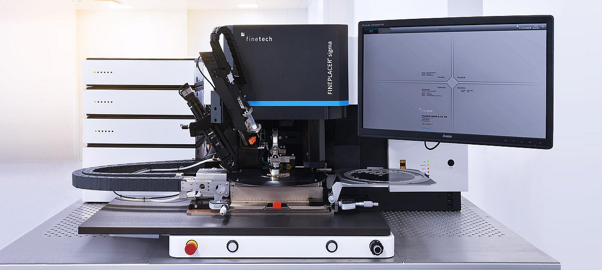
FINEPLACER® sigma
Unrivaled Flexibility for Research & Prototyping
"We use the FINEPLACER® sigma for a variety of applications, ranging from simple chip-to-submount to complex module assemblies with very high accuracy requirements. Easy manual operation makes the system also an ideal fit for low-quantity research samples."

Lars Schellhase
Ferdinand-Braun-Institut

Your Sales Contact
Thomas Müller
- Finetech GmbH & Co. KG
- Head of Sales Europe
- +4930936681300
- finetech_thomas
Contact Us

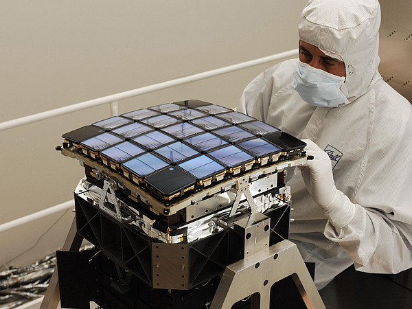
Focal Plane Array (FPA)
A Focal Plane Array (FPA) is a sensor with a two-dimensional detector pixel matrix, i.e. for infra-red light or X-rays, positioned in the focal plane of an optical system.

Eutectic Bonding with Au/Sn
Eutectic Gold/Tin (Au/Sn) is a hard solder alloy often used to bond demanding microelectronic and optoelectronic devices. They are available in different forms, such as pre-forms, solder paste or ribbons.
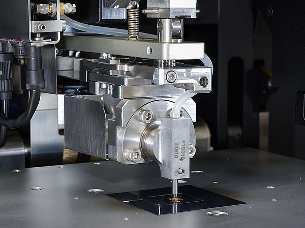
Ultrasonic Die Bonding
Ultrasonic / thermosonic bonding is a process primarily used for bond wires but also for flip chip bonding. Ultrasonic allows to generate a mechanically and electrically stable connection.
